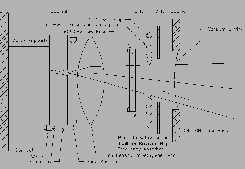
A bolometer is basically an absorber with some heat
capacity, connected to a cryogenic reservoir by a heat leak of chosen thermal
conductance. Changes in the incident power produce changes in the temperature
of the absorber. These changes in the temperature of the absorber are converted
to voltage using a current bias thermistor. Because the bolometers are
sensitive to a wide range of frequencies it is necessary to filter the
incoming radiation before it reachs the detectors (Figure ![[*]](cross_ref_motif.gif) ).
).
Figure:The filter structure of Bolocam. The horn array showed in the diagram is neccesary to coupling the radiation to the detectors increasing the sensitivity of the camera.
 |
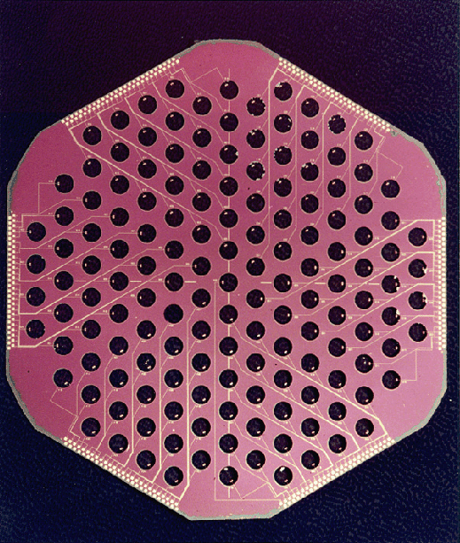
Bolocam is an bolometer array of 144 detectors (pixels)
(Figure ).
Each individual pixel is a spider web structure (see Figure )
made of metalized Silicon Nitride (Si3N4).
This grid is design to have an optimal absorption, rigid mechanical support
and minimize the cosmic ray cross section (Glenn et al. 1998). The thermistor
situated in the center of the structure consisting in a neutron-transmutation-doped
Germaniun (NTD Ge). This sensitive thermistor detect the changes in temperature
of the absorber due to changes in the incident radiation.
Figure:Individual micromesh
bolometer fabricated in the Center for Space Microelectronics and Technology
at JPL. The absolved is thermally isolated by radial legs of Silicon Nitride.
These legs are 5 ![]() m
m ![]() 1
1 ![]() m
in cross section. The Germaniun thermistor is
m
in cross section. The Germaniun thermistor is
connected to the grid through Indium
pads [From Bock et al. (1998)].
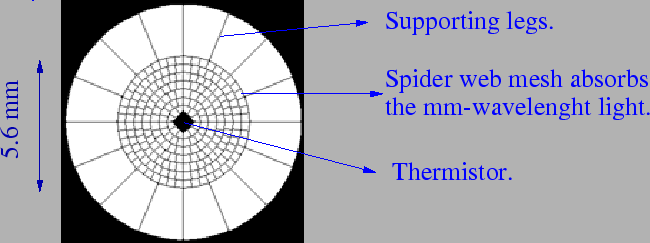 |
Figure:The 144 components
of the Bolocam array system. The wafer is 76 mm in diameter and 200 ![]() m
thick. Gold tracers connect each individual pixel with the conectors at
the edge of the wafer.
m
thick. Gold tracers connect each individual pixel with the conectors at
the edge of the wafer.
 |