The Kutsari National Semiconductor Design Center project was presented to the INAOE community
On Monday, February 3rd, the Kutsari National Semiconductor Design Center project was presented to the research and technological development community of the National Institute of Astrophysics, Optics, and Electronics (INAOE), a public center coordinated by the Secretariat of Science, Humanities, Technology, and Innovation (SECIHTI).
The meeting was chaired by Dr. Feliú D. Sagols Troncoso, Director General of Public Research Centers and National Laboratories at SECIHTI; Dr. David Sánchez de la Llave, Interim Director General of INAOE; Dr. Pascual Ogarrio, Director of Coordination of Public Research Centers; and Dr. Edmundo Gutiérrez Domínguez, Interim Director General of Innova Bienestar de México and national coordinator of the project.
Dr. Feliú Sagols said the meeting's objective was to provide information about the Kutsari project and its importance for Mexico's development and the positioning of INAOE.
He recalled that on February 6, Mexican President Dr. Claudia Sheinbaum Pardo announced the creation of the "Kutsari" National Semiconductor Design Center, which seeks to strengthen the country's semiconductor value chain, contributing to the industry and the economy, and making Mexico a scientific and technological power.
He added that the project will be supported by national HCTI policy, the semiconductor research in Mexican institutions, and capabilities in Jalisco, Puebla, and Sonora, among other states.
He added that in terms of installed capacity and scientific infrastructure, INAOE has cutting-edge areas of expertise, including integrated circuit design. It also has laboratories, a clean room, and scientific promotion and outreach activities.
He said that INAOE's capabilities will contribute to the Kutsari project, becoming a benchmark for institutions in the HCTI sector.
Regarding its operation, he reiterated what Dr. Rosaura Ruiz Gutiérrez had stated on February 6 that Kutsari entails the creation of a design center with immediate commercial viability and, in the medium term, a manufacturing center.
The project requires, in its initial stage, addressing aspects such as a legal and regulatory framework to strengthen the development and transfer of technology in the field; an ecosystem that includes the entire supply chain in development centers; incentives for technological production in semiconductor electronics; and leveraging the experience of Mexican scientists and technologists.
In a second phase, Dr. Sagols explained, the project requires beginning the manufacturing of traditional or legacy chips to transfer domestic demand to the home appliance, automotive, medical equipment, sensor, and other strategic device industries.
Finally, he said that the project represents an opportunity to join the integrated circuit design and manufacturing ecosystem and to provide Mexico with viable opportunities to become a player in this technological sector, which is in global competition for strategic and commercial reasons.
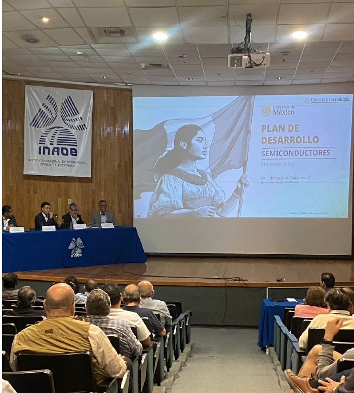
For his part, Dr. Edmundo Antonio Gutiérrez Domínguez presented the semiconductor development plan, the goal of which is to consolidate development capabilities in Mexico by creating a design center with immediate commercial viability and, in the medium term, a manufacturing center with a strategic vision.
As context, he noted that the COVID-19 pandemic triggered a logistics crisis in the chip and other semiconductor supply chain. Therefore, Mexico, through various Ministries and Institutions, as well as the United States and Canada, have been working together to relocate the semiconductor industry in the region, leveraging the capabilities of the three countries.
Specifically, he added that "Kutsari" is based on the design capabilities of the country, which for more than four decades has invested in research, development, and highly trained personnel at INAOE, CINESTAV, UNAM, IPN, and other higher education institutions. Market opportunities encompass industry and the strategic sectors of telecommunications, IR sensors, and satellites. He emphasized that design across the full range of technologies is possible in Mexico.
To achieve this, it is necessary to develop a public policy that integrates a program for the development of the semiconductor industry aligned with Plan Mexico, the creation of a 100% publicly owned design center, and the definition of a semiconductor manufacturing model, which could be public, private, or mixed, by 2026.
Luis Enrique Erro # 1, Tonantzintla, Puebla, México, Código Postal 72840, Tel: (222) 266.31.00, difusion@inaoep.mx
This work is licensed under a Creative Commons Attribution-NonCommercial-NoDerivs 2.5 Mexico License.
