With cutting-edge equipment, the Electron Microscopy Laboratory of INAOE stands as a unique facility in southern Mexico
Santa María Tonantzintla, Puebla, February 4, 2025. With the acquisition and installation of cutting-edge equipment, the Electron Microscopy Laboratory of the National Institute of Astrophysics, Optics and Electronics (INAOE), a center of the Secretariat of Science, Humanities, Technology and Innovation (Secihti), stands as a unique facility in the southern region of our country, as it provides service to researchers and students of INAOE and other institutions in the area.
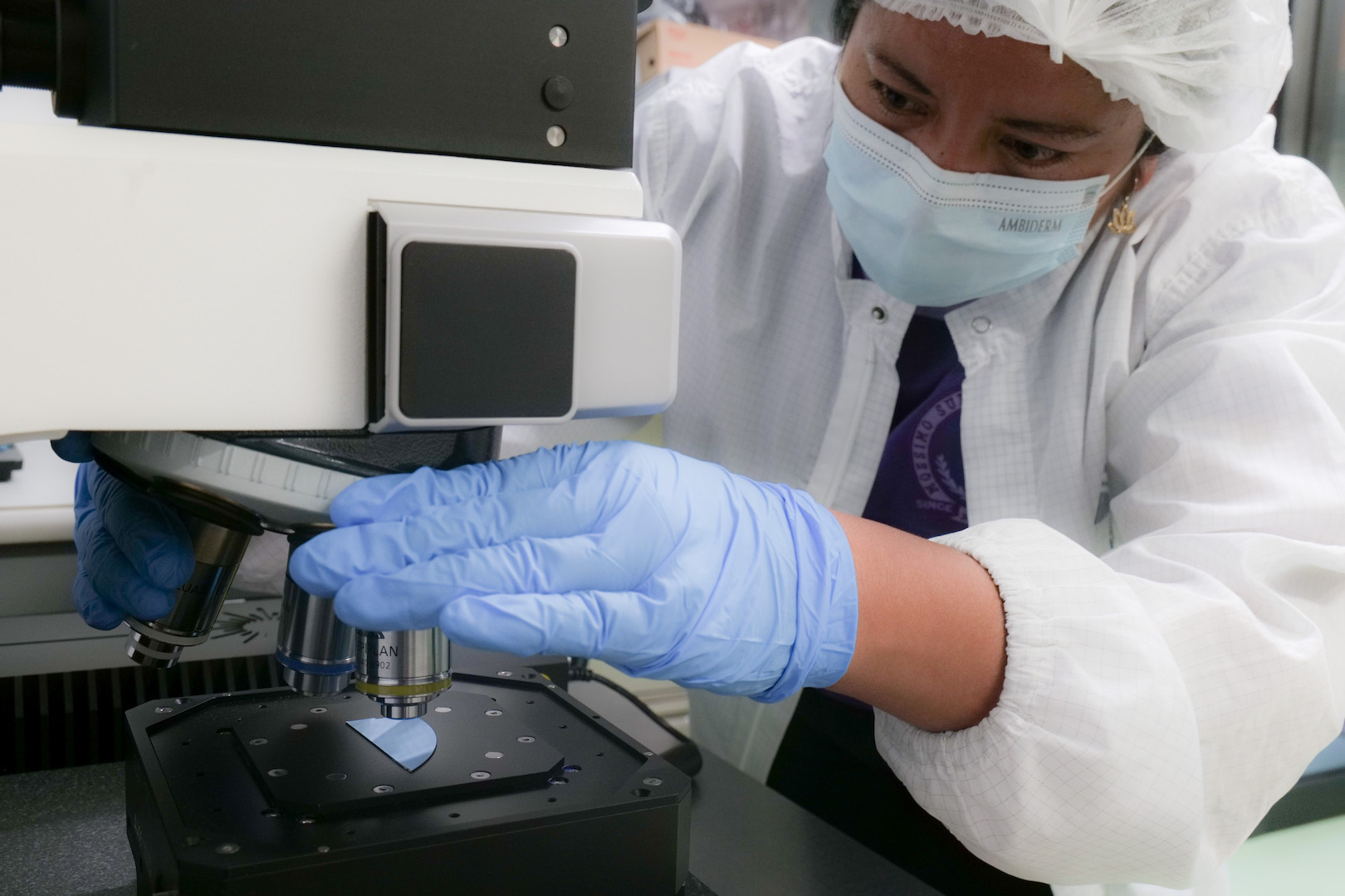
With the acquisition of a new transmission electron microscope (TEM), the laboratory now has three electron microscopes, two of them scanning electron microscopes (SEM) that, by using electron beams, have very high resolutions that are in the order of nanometers in the case of SEM microscopes, and in the order of angstroms in the case of TEM. These microscopes are used for the characterization of nanomaterials and semiconductor devices developed in research projects.
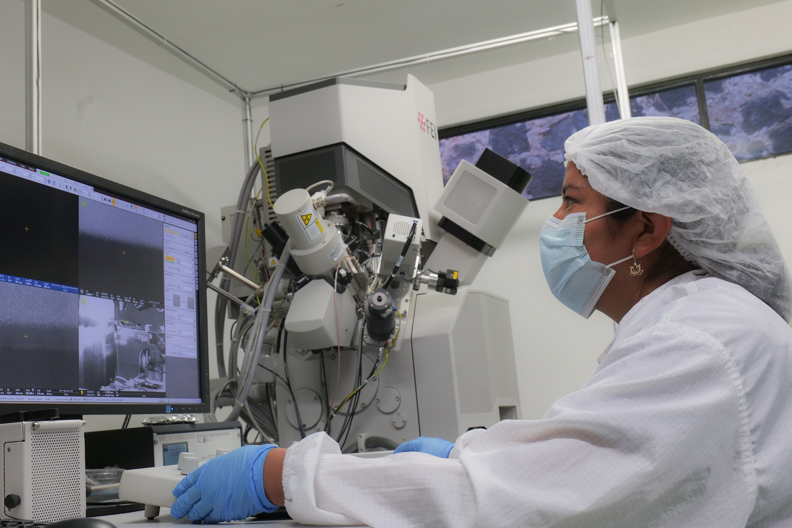
The history of the Electron Microscopy Laboratory of INAOE, explains Dr. Mario Moreno Moreno, INAOE researcher and head of the laboratory, can be divided into two stages. The first was inaugurated in 2016, when the laboratory was equipped with a FEI scanning electron microscope model SCIOS, which is used to analyze devices and nanomaterials at a resolution of less than one nanometer and which has two columns (DUAL BEAM): one for electrons and one for ions (FIB). This second column is used to observe the surface, and also the layers that comprise it transversally. It also enables nanofabrication, that is, nanometric devices can be made. At this period, a Hitachi SU3500 scanning electron microscope was also acquired.
Dr. Moreno says: “The Electron Microscopy Laboratory was founded in 2016. In addition to the two microscopes, the equipment was integrated with a Raman microscope to characterize films and determine the crystalline fraction in the different nanomaterials that we use. We also have a Fourier transform infrared spectrometer (FTIR) and an atomic force microscope. This was the first stage of the laboratory.”
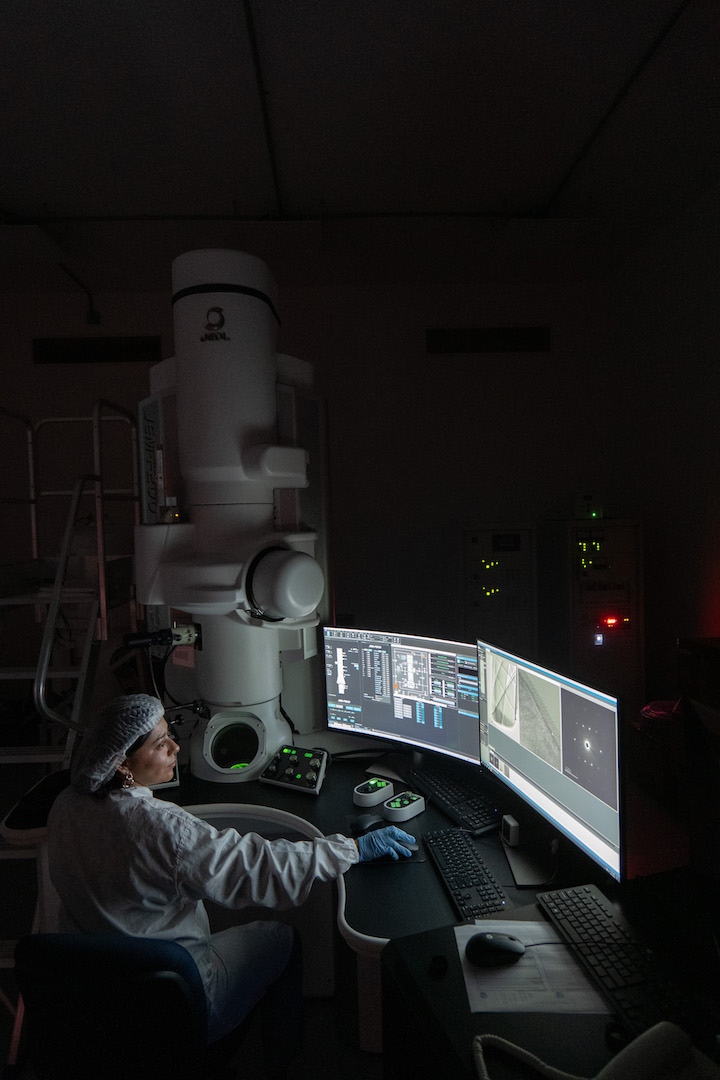
The second stage arose through a project of the Electronics Coordination with which a Jeol brand transmission electron microscope, model JEM-F-200, was acquired. To house this large-scale equipment (it is almost three metres high), an additional laboratory was built in front of the first stage.
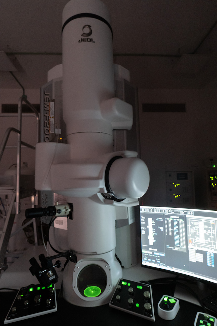
“The space is very specialized: to avoid vibrations, the floor is a thick cement slab, and it is kept at a constant temperature of 19 degrees. It has air conditioning and a machine room.”
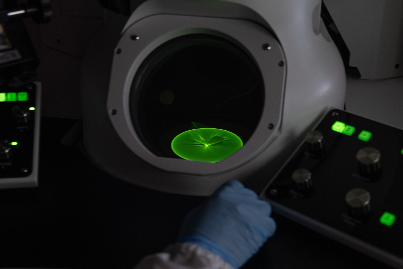
The new microscope has a very high resolution of 1.4 angstroms, explains the researcher, adding: “It is a cold emitter, so the electron beam has less dispersion, which allows greater resolution. Additionally, it can perform elemental chemical analysis using two energy dispersion spectrometers (EDS), and various elements can be detected. For example, in a silicon sample, we can determine if it is contaminated with oxygen, carbon, phosphorus, etc. The microscope allows us to chemically detect the elements in the samples.”
As a cold emitter microscope, it allows for greater resolution: “Thanks to this microscope, crystalline substrates such as crystalline silicon wafers or nanocrystals in films that are generally amorphous with nanocrystals included can be observed practically in atomic order.”
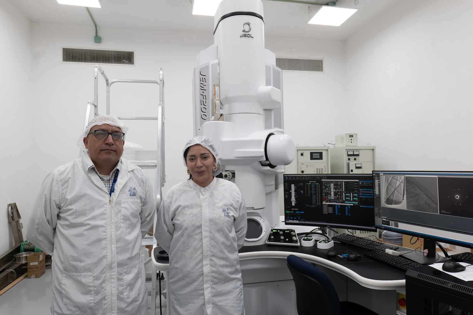
With this microscope, Dr. Moreno points out, the laboratory is very complete and, from Puebla to the south and southeast of Mexico, there is nothing like it: “We are proud of this laboratory that arose from the need to analyze nanostructured and nanocrystalline semiconductor materials that have been developed in our semiconductor manufacturing laboratories for several years, but we did not have the tools to analyze and observe them. The laboratory gives a plus to everything that is done in terms of manufacturing. This equipment helps us analyze the structure of the material and see properties such as the chemical composition or roughness that we analyze with the atomic force microscope, the crystalline fraction with the Raman microscope. It helps us to characterize materials in many ways.”
For more information contact Mario Moreno: mmoreno@inaoep.mx
Luis Enrique Erro # 1, Tonantzintla, Puebla, México, Código Postal 72840, Tel: (222) 266.31.00, difusion@inaoep.mx
This work is licensed under a Creative Commons Attribution-NonCommercial-NoDerivs 2.5 Mexico License.
